Characteristics of X-ray
absorption near-edge spectra obtained from various MgB2 films
C. H. Hsieh1, C. N. Chang1, S. Y. Wang1, Pohan Lee2, H. C. Hsu1, Y. Cui3, X. X. Xi3, Eun-Mi Choi4, Sung-Ik Lee4, and J. M. Chen5
1. Department of Physics,
2. Department of Physics,
3. Department of Physics, Pennsylvania State University, University Park, Pennsylvania 16802, U. S. A.
4.
5.
X-ray absorption near-edge spectrum (XANES) of various MgB2 films prepared under different procedures has been measured by using synchrotron radiation. By comparing to the band structure calculation we observed that the major spectral peaks of B K edge XANES resulted from the empty states with p characters of boron in MgB2. The spectral peak near the threshold indicates the existence of the hole states in the valence band at the Fermi level. This is particularly clear in some c-axis oriented films. The peaks of B2O3 were common peaks in all of the films we studied, indicating the contamination of B2O3. This peak sometimes will smear the main spectral structure of MgB2 if it is seriously contaminated.
The experimental XANES of Mg K edge results from the empty states with Mg p characters can be identified by comparing the experimental spectrum with the band structure calculations. A small core-hole effect resulted from the less electron screening of the Mg ions in MgB2 can be identified. There are empty states, as appear in the threshold spectral structure, extended from the Fermi level indicates the metal characters of Mg in MgB2. Little anisotropic characteristics between px,y and pz can be identified from the polarization-dependent measurements, except the spectral intensity around 1314 eV. Around that energy, the spectral intensity is higher for the electric field of the beam parallel than perpendicular to the boron planes, in accordance with the band structure calculations.
I. Introduction
Since the discovery of the superconductivity of MgB2 [1], many works have been done for understanding the precise mechanism of its record-high value of the superconducting temperature (〜 40 K) among the binary intermetallic compounds.
It is known that MgB2 is a metal with a layer structure with alternating layers of boron and magnesium atoms. The boron atoms form honeycombed layers similar to the layers of graphite, with covalent, sp2 hybridization bonds (�m - bonds) and the pz bonds (�k - bonds). The magnesium atoms are located above the center of the hexagons in-between the boron planes. The magnesium atoms will transfer charges to boron atoms for having enough electrons to form the �m - bonds and �k- bonds. In fact the electronic structure calculated on the basis of a fictional system ��2+B2 is very similar to that of MgB2 [2], except that �m - bonds, as in graphite, are completely filled. The graphite becomes superconducting up to 5K when doped (intercalated) [3]. Several different ab initio band calculations show that the �m - bonds and �k - bonds of MgB2 are not completely filled at the Fermi level [2, 4-7]. The energy position of the B �m(2px,y) bands at the point of Brillouin Zone lie above the Fermi level and form hole-type cylindrical elements of the Fermi surface [8]. The B 2pz states are oriented perpendicularly to the boron plane and responsible for the weak interlayer �k bonds. Both �m and �k bands of B are suggested to be critical for the description of the mechanism of the superconductivity of MgB2 [8, 9].
One also notices that magnesium states in MgB2 are important to understand the charge transfer mechanism of Mg to B. A hybridization of B 2pz level and Mg 2p level will lower the former while raising the latter. This hybridization effect lowers the �k(pz) bands relative to the bonding �m bands and cause �m �� �k charge transfer and hole doping in �m band, deriving the superconductivity in MgB2 [2].
The unoccupied states with p character close to the Fermi level can be easily probed by the K X-ray absorption near-edge spectrum (XANES) because of the dipole transition rule. By using the technique of X-ray absorption spectroscopy on films of MgB2 one can look into the partial density of states (PDS) above the Fermi level. If the film has c-axial oriented crystalline structure one can use polarized X-ray to probe the PDS parallel to the boron/magnesium planes (ab plane) and perpendicular to the planes. In other words, one can probe the empty states of px,y and pz.
Nevertheless, fabricating films of MgB2 is not an easy task since MgB2 is not easily stabilized substances. Contaminations will attribute to the characteristics of the XANES of MgB2 films. We report our study of various films of MgB2 fabricated by different method by XANES and show that the main characteristics of the XANES disturbed little by the contaminations. The characteristics of XANES indicate the characteristics of the PDS (the electronic structure) of MgB2.
II. Experiments
A. Samples
The MgB2 films used in this work
were made by different methods: Samples S1 and S2 that were obtained by
post-annealing a precursor film made by ion sputtering a Mg-rich MgB2 target on
a substrate of R-plane Al2O3 single crystal in either an
oxygen-free copper cell (for S1) or an ultra-high vacuum comparable stainless
steel cell (for S2) under magnesium vapor at about
B. X-ray absorption near edge spectra (XANES)
Our soft X-ray absorption spectra were measured at room temperature at
the beam line
The experimental geometry is indicated in Fig.2, where the normal n of the ab plane of the film is indicated. The photon detector is a multichannel plate (MCP) that is sited at 45�X with respect to the incident beam (�hin) to detect the outgoing X-ray fluorescence (�hout). In other words, we use a bulk sensitive total-fluorescence-yield (TFY) method for obtaining the soft X-ray absorption near�Vedge spectra (XANES). Simultaneously, the sample current signal is collected. This signal measures the photoelectrons coming out of the sample by the impact of photons. It is a total-electron yield (TEY) method for the XANES. The spectrum obtained by the TEY is surface sensitive due to the short mean free path of the outgoing electrons created by the impact of photons in the sample. The intensity of the incident photons was measured by the current generated by a fresh nickel mesh located in front of the target chamber. By rotating the sample holder we can scan the polarization vector parallel to the ab plane toward to the c-axis by varying the angle �\ from 0�X to 75�X. Note that the normal n will pass the line of �hout for �\��45�X and the angles �\ and �] are on the same side of normal n.
The energy of the XANES of boron K edge was calibrated by referring to the resonance peak of B2O3 to be 193.8 eV, while that of Mg K edge was calibrated by referring to the energy at the inflection point of the K edge of Mg metal to be 1303.0 eV. Each spectrum was normalized with the intensity of the incident photons.
The target self-absorption was not corrected. It is proper for the XANES of Mg K edge since the mean free path of the photons there is about 1.2 �gm, much greater than the target thickness and therefore, the target self-absorption effect can be neglected. The XANES of B K edge may be distorted due to target self-absorption effect since the mean free path of the photons there is about 100 nm smaller than the target thickness that is about 400 nm to 700 nm for the samples we studied. The resonance peak may be suppressed due to a larger self-absorption effect. Besides, the self-absorption effect is also angular dependent [14], which will affect the overall spectral features. Nevertheless, the resonance spectral positions will not be altered. It is difficult to do the self-absorption correction for samples contain impurities. The uncorrected spectrum will not affect the conclusions of this work as will be shown later.
III. Results and Discussions
(A) General features of the XANES
Fig.3 shows the XANES of B K edge for all samples. They were taken at �\ = 45�X. The spectrum of B2O3 is included for comparisons. Both TFY (Fig.3 (a)) and TEY spectra (Fig.3 (b)) are shown. The peaks resulting from B2O3 (the peak D at 193.8 eV) is seen in all samples, it is relatively clear in the TEY spectra. The peak C (191.9 eV) is relatively pronounced in S1. The origin of this peak is not so clear; it had been suggested to be from the inelastic resonance scattering [15] or some kind of surface contaminations [16]. This peak seems to smear out the other peaks, such as peaks A (186.7 eV), B (189.4 eV), and E (210 eV) , which are thought to be the peaks resulting from MgB2 and clearly shown in the other samples. A broad spectral peak between about 195 eV to 205 eV is clearly observable in both S3 and S4.
Fig.4 shows the XANES of Mg K edge for all samples. They were taken at �\ = 45�X. The spectrum of MgO is included for comparisons. Both TFY (Fig.4 (a)) and TEY spectra (Fig.4 (b)) are shown. MgO contains three peaks located at b (1310.8 eV), d (1318 eV) and f (1329.4 eV). The peak a (1304.3 eV), c (1314.3 eV), and e (1325.4 eV) will be the peaks resulting from MgB2 if the major impurities of the sample is MgO and B2O3. One notices that S1 and S2 contain great amount of MgO, while S3 and S4 contain little.
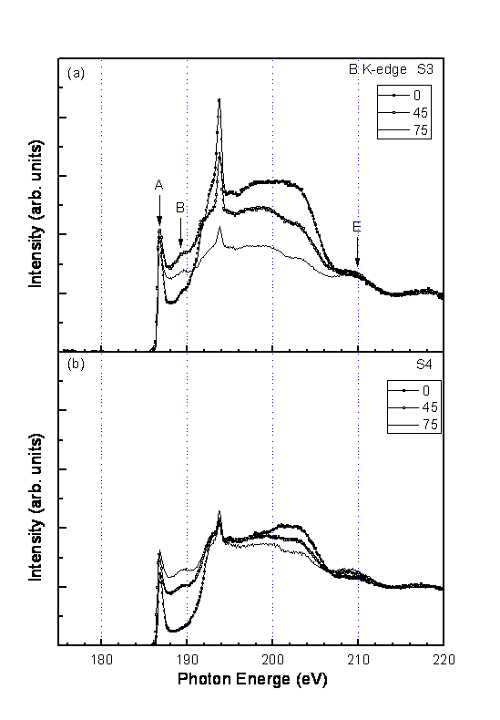
(B) The polarization dependent XANES of S3 and S4
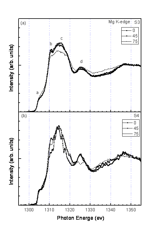
The polarization dependent XANES of S3 and S4 are shown in Fig.5 and Fig.6 respectively for B K edge and Mg K edge. These spectra are further normalized such that the relative spectral height of the high energy portion to the spectral height below the threshold is the same.
In the XANES of B k edge (Fig.5), the change of the threshold peak A
from �\ = 0�X to �\ = 75�X is mild, while the increase of the spectral intensity of the peak
B is apparent. The broad peak between about 195 eV and 205 eV decreases from �\ = 0�X to �\ = 75�X. These
variations reveal the anisotropic nature of the electronic structure since the
polarization vector of the probe beam is parallel to the ab plane of MgB2
films at �\ = 0�X and varies toward parallel to the c-axis by increasing the
angle �\ to 75�X. Therefore, one probes the boron px,y(�m) at �\
= 0�X and the pz(�k) states at �\ =
90�X. The experimental arrangement at �\ = 90�X is not possible due to the finite
size of the detector and the block of the outgoing X-ray florescence by the
target itself. The measurement at �\ = 75�X is considered to be have most
information result from the boron pz(�k)
states.
The peak A is the sole peak for �\ = 0�X up to about 4 eV from the threshold. Its width is about 0.6 eV. The peak position is at 186.7 eV. The appearance of this peak as well as other features of our spectra at different scan angles is in agreement with that reported by Zhang et al. [17], but in disagreement with the data shown by Cepek et al. [18], in which the peak A was not observed. The peak B increases for the increase of the scan angle �\. Since there is no peak B observable at �\ = 0�X, we suggest that the peak B results entirely from the planes parallel to the c axis of the sample, corresponding to the boron pz bonds (�k bonds).
In the XANES of Mg K edge (Fig.6), the anisotropic feature is much less apparent than what appears in the XANES of B Kedge. The existence of empty states starting 1304 eV is apparent. It indicates the metal-like nature of the Mg ions in MgB2.
(C). Comparisons of the XANES and Band structure calculations
The partial density of states (PDS) for boron px,y(�m) and pz(�k) states obtained by various band calculations, either based on the full potential augmented plane wave method (FLAPW) [16,19,20] or based on the other methods [21,22] are similar and always shows that there are two degenerated states in the boron �m band crossover the Fermi level (without core hole and will be referred to as the ground-state PDS). We compare our spectra with the ground-state PDS calculated by the augmented plane waves plus local orbitals (APW+lo) method, encoded in the WIEN 2K software [23], up to the energy 30 eV above the Fermi level in Fig.7 and Fig.8. Lattice parameters of a = 3.089 Å and c = 3.522 Å, and muffin-tin radii of 2.91 au for Mg and 1.68 au for B were used in the calculation. For clarity only the spectra of 0�X (Fig.7) and 75�X (Fig.8) of S4 are shown for comparisons. The corresponding binding energies measured from the Fermi level are given in the lower scale for both figures. The Fermi level measured from 1s core level of both the XANES of B K edge and Mg K edge is taken to be the inflection point of the threshold peak (peak A for boron and peak a for magnesium). This assignment is in accordance with the X-ray absorption and X-ray emission study [24] for B K edge in MgB2.
Fig.7 shows the combination drawing of the XANES of both B K edge and Mg K edge at �\ = 0�X and the PDS with px,y characters in the band structure calculations. The agreements between experiment and theory are very well, although a small energy shift is visible for the XANES of Mg K edge. This spectral shift toward the low energy can be caused by the core-hole effect [25] since Mg in MgB2 is a partially ionic atom, the interaction of the core-hole potential in the X-ray absorption process can be effective due to less electron screening of the Mg ions.
The peak A thus indicates the narrow hole states in the B �m(2px,y) bands lie just above the Fermi level in the valence band. This interpretation is in accordance with recent reports that showed the threshold peak intensity (peak A in our case) in the boron K- edge X-ray absorption spectra of Mg1-xAlxB2 decreased with the increase of Al doping up to about x = 0.3, consistent with hole filling of the �m band crossover the Fermi level [26, 27]. The hole filling caused the detriment of the superconductivity. Our assignment is also in agreement with the recent report by Klie et al. in using EELS [28], in which the peak A was also demonstrated to have px,y character.
The metal-like PDS with px,y characters is revealed by the XANES of Mg K edge. The empty band with px,y characters around the binding energy of about 13 eV is indicated by the broad peaks in the XANES of B K edge ( around 198.5 eV) and Mg K edge (around 1314 eV). Both the peak E and the peak d indicate the band around the binding energy of 22.5 eV. It is clearly shown in this combination drawing that these bands are mixing bands of boron states and magnesium states in MgB2.
Fig.8 shows the combination drawing of the XANES of both B K edge and Mg K edge at �\ = 75�X and the PDS with pz characters in the band structure calculations. The agreements between experiment and theory are good even though the spectra contain some contribution from the states with px,y characters at �\ = 75�X (rather than �\ = 90�X). One specially notes that the peak B reveals the PDS with pz characters in the band calculations around the binding energy of 3.0 eV. The threshold peak indicates there are hole states near the Fermi level. The appearance of this spectral peak to be shaper than the prediction of the band structure calculation could be due to the contribution from the px,y states. The spectral energy shift is also shown in the XANES of Mg K edge which again is due to the core-hole effect caused by the less electron screening of the Mg ions.
IV. Conclusions
In this work we show that the X-ray absorption near-edge spectrum (XANES) of MgB2 provides information of the electron structure of the empty states above the Fermi level, although the sample may have some impurities, namely B2O3 and MgO. The threshold peak of the XANES of B K edge (peak A in Fig.2 and Fig.6) indicates the narrow hole states in the B �m(2px,y) bands lie just above the Fermi level. The second peak of the XANES of B K edge (peak B in Fig.2 and Fig.7) indicates empty states with pz characters about 3.0 eV about Fermi level. The experimental XANES of Mg K edge results from the empty states with Mg p characters can be identified by comparing the experimental spectrum with the band structure calculations. A small core-hole effect resulted from the less electron screening of the Mg ions in MgB2 can be identified. There are empty states, as appear in the threshold spectral structure, extended from the Fermi level indicates the metal characters of Mg in MgB2. Little anisotropic characteristics between Px,y and pz can be identified from the polarization-dependent measurements of the XANES of Mg K edge.
Acknowledgement
This work is partially supported by the
National Science Council of the Republic of China under grant No. NSC
92-2112-M-003-012. The full support of the staff at the National Synchrotron
Radiation Research Center (NSRRC) is greatly appreciated. The work at
References:
1. J. Nagamatsu, N. Nakagawa, T. Muranaka, Y. Zenitani, and J. Akimitsu, Nature 410, 63-64 (2001)
2. J. M. An, and W. E. Pickett, Phys. Rev. Lett. 86, 4366-4369 (2001)
3. I. T. Belash, A. D. Bronnikov, O. V. Zharikov, and A. V. Palnichenko, Solid State Commun. 64, 1445 (1987)
4.
I. R. Shein, N. I. Medvedeva,
and A. L. Ivanovskiĭ, Phys.of the
5. K. D. Belashchenko, M. van Schilfgaarde, and V. P. Antropov, Phys. Rev. B64, 092503 (2001)
6. M. J. Mehl, D.A. Papaconstantopoulos, and D. J. Singh, Phys, Rev. B64, 140509(R) (2001)
7. K. Kokko, V. Kulmala, and J. A. Leiro, Phys. Rev. B66, 165114 (2002)
8. Hyoung Joon Choi, David Roundy, Hong Sun, Marvin L. Cohen & Steven G. Loule, Nature 418, 758 (2002)
9. H. Rosner, J. M. An, W. E. Pickett, and S. L. Dresheler, cond-mat/0203030 (2002)
10. W. N. Kang, Hyeong-Jin Kim, Eun-Mi Choi,
C. U. Jung, Sung-Ik Lee, Science 292, 1521(2001)
11. Xianhui Zeng, Alexej V. Pogrebyakov, Armen
Kotcharov, James Jones, X. X. Xi, Eric M. Lysczek, Joan M. Redwing, Shengyong
Xu, Qi Li, James Lettieri, Darrell G. Schlom, Wei Tian, Xiaoqing Pan and Zi-Kui
Liu, Natural Materials 1, 1 (2002)
12. Liang-Yann Wu, Chu-Nan Chang, Chi-Hsiang, Bin-Jou Huang, Hong-Chang Yang, and Jin-Ming Chen, Chinese J. of Phy. 42, 534(2004)
13. 13. S. -C. Chung, C. �VI. Chen, P. �VC. Tseng, H. �Vf. Lin, T. �VE. Dann, Y. �VF. Song, L. �VR. Huang, C. �VC. Chen, J. �VM. Chang, K. �VL. Tsang, and C. �VN. Chang, Rev. Sci. Instrum. 66, 1655 (1995)
14. L. Tröger, D. Arvanitis, K. Baberschke, H. Michaelis, U. Grimm, and E. Zschech, Phys. Rev. B46, 3283(1992)
15. T. A. Callcott, L. Lin, G. T. Woods, G. P. Zhang, J. R. Thompson, M. Paranthaman, and D. L. Ederer, Phys. Rev. B64, 132504(2001)
16. Y. Zhu, A. R. Moodenbaugh, G. Schneider, J. W. Davenport, T. Vogt, Q. Li, G.. Gu, D. A. Fischer, and J. Tafto, Phys. Rev. Lett. 88, 247002(2002)
17. G. P. Zhang, G. S. Chang, T. A. Callcott, D. L. Ederer, W. N. Kang, Eun-Mi Choi, Hyeong-Jin Kim, and Sung-Ik Lee, Phys. Rev. B67, 174519 (2003)
18. C. Cepek, R. Macovez, M. Sancrotti, L. Petacci, R. Larciprete, S. Lizzit, and A. Goldoni, App. Phys. Lett. 85, 976(2004)
19. N. Jiang, B. Jiang, J. C. H. Spence, R. C. Yu, S. C. Li, and C. Q. Jin, Phys. Rev. B66, 172502-1(2002)
20. X. Kong, Y. Q. Wang, H. Li, X. F. Duan, R. C. Yu, S. C. Li, F. Y. Li and C. Q. Jin, App. Phys.Lett. 80, 778 (2002)
21. J. A. Leiro, K. Kokko, and V. Kulmala, J. of Alloys and Compd. 362, 139(2004).
22. I. R. Shein, N. I. Medvedeva, and A. L. Ivanovskiĭ, Physics of the solid state, 43, 2213(2001)
23. K. Schwarz, P. Blaha, and G. K. H. Madsen, Comput. Phys. Commmun. 126, 71(2002)
24. Jin Nakamura, Nobuyoshi Yamada, Kazuhiko Kuroki, Thomas A. Callcott, David L. Ederer, Jonathan D. Denlinger, and Rupert C. C. Perera, Phys. Rev. B64, 174504(2001)
25. F. de Groot, Chem. Rev. 101, 1779(2001)
26. K. �VD. Tsuei, H. �VJ. Lin, L. �VC. Lin, T. �VY. Hou, H. H. Hsieh, C. T. Chen, N. L. Saini, A. Bianconi, and A. Saccone, Int. J. Mod. Phys. B16, 1619(2002)
27. H. D. Yang, H. L. Liu, J. �VY. Lin, M. X. Kuo, P. L. Ho, J. M. Chen, C. U. Jung, Min-Seok Park, and Sung-Ik Lee, Phys. Rev. B68, 092506(2003)
28. R. F. Klie, Y. Zhu, G. Schneider, and J. Tafto, App. Phys. Lett. 82, 4316(2003)
Figure Captions
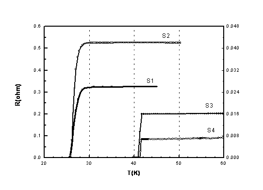
Fig.1. The temperature dependent resistances of the samples: the right scales are for S1, S2, and S3, and the left scales are for S4.
Fig.2. Top view of the experimental geometry. A linear polarized photon beam with frequency �hin is incident on the sample and the frequency of the outgoing X-ray fluorescence is �hout. n is the surface normal(c-axis). E is the polarization of the incident beam.
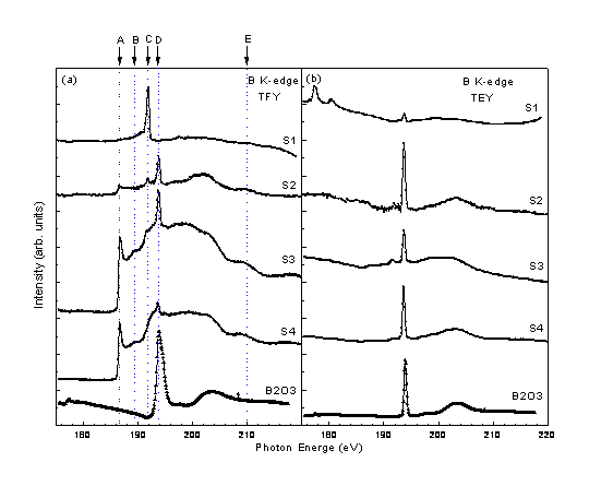
Fig.3. The XANES of B K edge of the samples from (a) TFY measurement and (b) TEY measurement
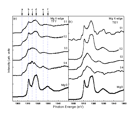
Fig.4. The XANES of Mg K edge of the samples from (a) TFY measurement and (b) TEY measurement
Fig.5. The polarization dependent XANES of B K edge of the c-axis orientation samples S3 and S4 at �\ = 0�X, 45�X, and 75�X. The spectra have been normalized such that the relative spectral height at high energy portion (around 217 eV) to that below the threshold is the same.
Fig.6. Same as Fig.5 except for the XANES of Mg K edge.
Fig.7. The combination drawing of the XANES of both B K edge and Mg K edge at �\ = 0�X and the PDS with px,y characters in the band structure calculations by using WIEN 2K code.
Fig.8. Same as Fig.7 except for �\ = 75�X